
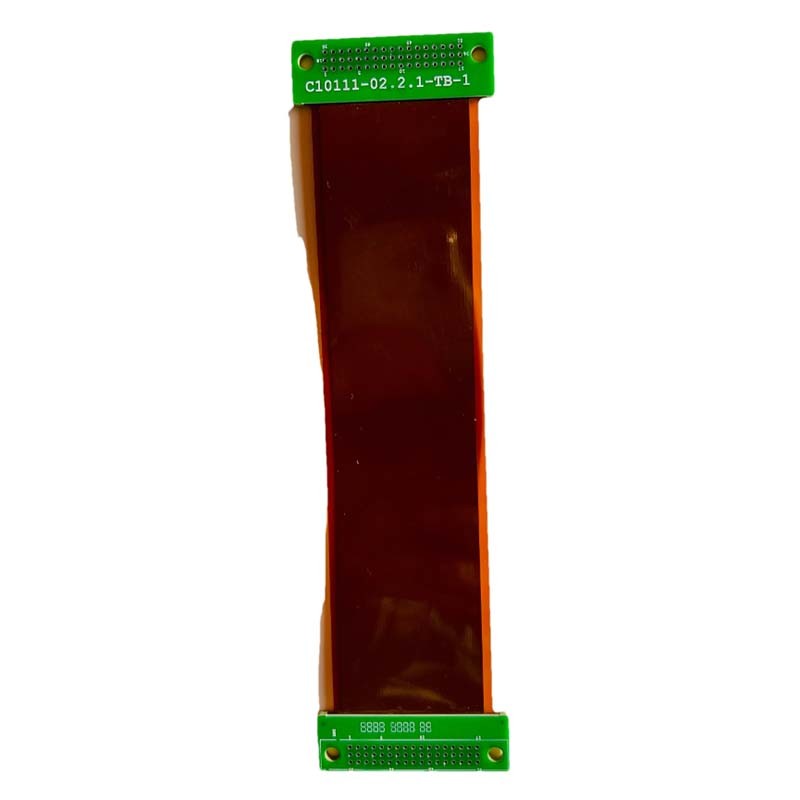

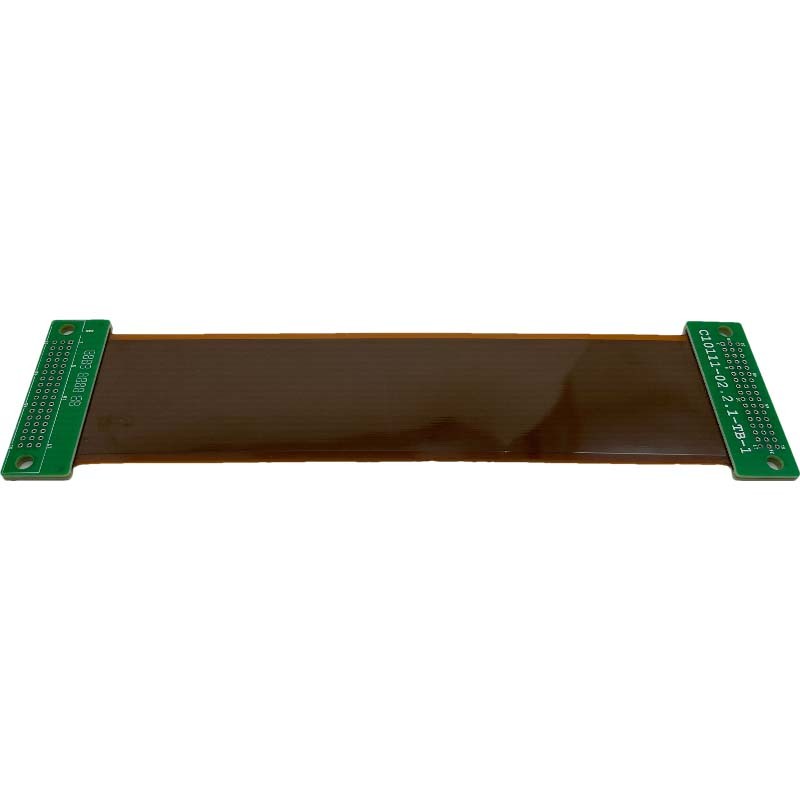
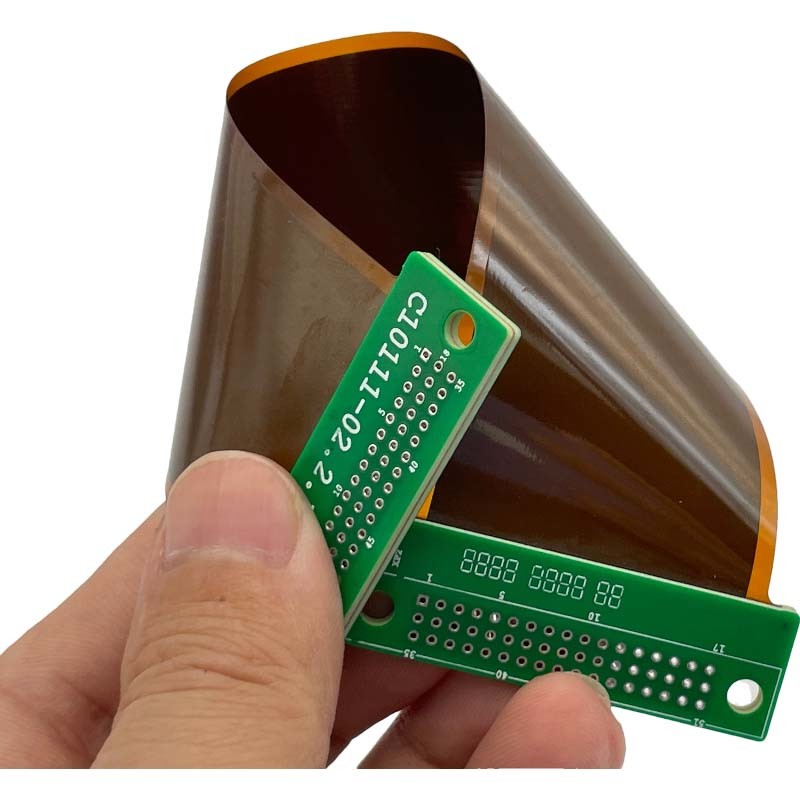
PCB flexible board, a type of flexible circuit board, can bend, fold, and wrap without affecting its performance. This type of circuit board is typically made from multiple layers of polyimide material (such as Kapton) and uses special techniques to print the wire pattern on the surface. Compared to traditional rigid circuit boards, PCB flexible boards can better adapt to complex three-dimensional spaces. Additionally, because this circuit board can be flexibly bent, it has widespread applications in industries such as medical devices, aerospace, automotive, and consumer electronics.
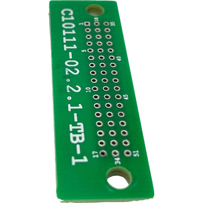
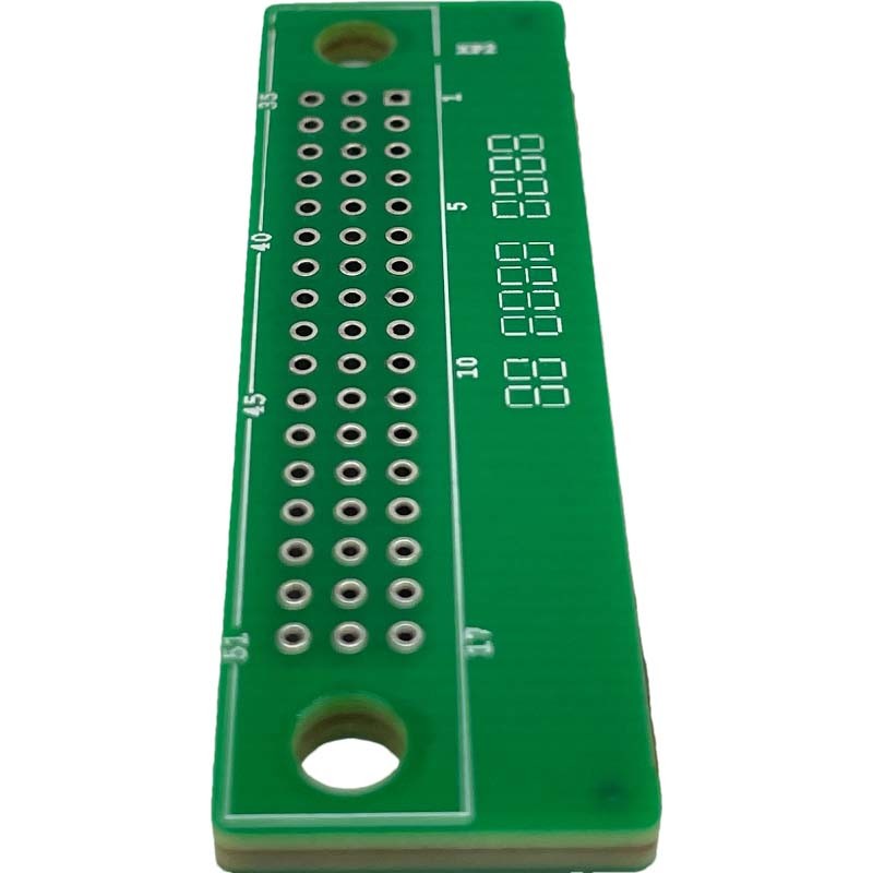
The manufacturing process of PCB flexible boards has strict requirements and technical points. During the manufacturing process, it is necessary to consider the physical properties and mechanical performance of the polyimide material, and to precisely control the process parameters such as temperature, humidity, and air pressure of the chemical treatment. Typically, the production process of this type of circuit board includes: raw material pretreatment, thin film layer sequencing, copper foil covering, photoresist coating, pattern exposure, chemical etching, drilling, metallization, final inspection, and other steps. In these processes, high-precision equipment and technology are required to ensure that the circuit board meets high-quality standards and has excellent mechanical and electrical performance.
| Standard Panel Size | 18″x24″ |
| Copper Thickness | 0.5 oz. To 6.0 oz. |
| Board Thickness | 0.5mm~3.0mm (0.02″~0.12″) |
| Minimum Height | 25 mil (0.64 mm) |
| Minimum Width | 6 mil (0.15 mm) |
| Solder Mask | White, Black, Blue, Green, Red |
| Legend/Silkscreen Color | Black, White |
| Surface Finishing | Immersion Gold, HASL, OSP |
| Layer | 1-40 Layers |
| Standards |
MIL-PRF-55110, MIL-PRF-50884, MIL-PRF-31032 UL94V.0, IPC-6012,6013, ISO-9001, AS910 |
| Turnaround Times | Multilayers: 1 to 5 days |
| Minimum Drill (Mechanical) Hole Diameter | .006″ (0.15 mm) |
| Minimum Micro Via (Laser) Size | 1 mil (0.025 mm) |
| Minimum Via (Laser) Size | 1 mil (0.025 mm) |
| Shielding Material | Copper, Silver Ink, Tatsuta, Carbon |
Global Well Electronic has a huge experience of more than 2 decades in the field of manufacturing different types of PCBs, including flexible, rigid, and rigid flex printed circuit boards. The team of experts at Rigiflex have a good knowledge of the circuit boards provided by the company, and can help you in selecting the right one based on your application requirements. All the PCBs provided by us are available at competitive prices. In addition to this, if you need circuit boards in a short time, we can assure quick delivery because we offer the fastest turnaround times in the industry. The rigid-flex printed circuit boards manufactured by us are sturdy and capable to withstand harsh environments.
1. PCB fabrication.
2. Turnkey PCBA: PCB+components sourcing+SMD and through-hole assembly
3. PCB clone, PCB reverse engineering.
PCB or PCBA Files Requests:
1. Gerber files of the bare PCB board
2. BOM (Bill of material) for assembly (please kindly advise us if there is any acceptablecomponents substitution.)
3. Testing Guide & Test Fixtures if necessary
4. Programming files & Programming tool if necessary
5. Schematic if necessary
![]()
| Order Quantity | 1-300,000,30000 Square Meter/Square Meters per Month module electronic board |
| Layer | 1,2,4,6,upto 40 layer |
| Material | FR-4,glass epoxy,FR4 High Tg,Rohs compliant,Aluminum,Rogers,etc |
| PCB type | Rigid,flexible,rigid-flexible |
| Shape | Any shape: Rectangular,round,slots,cutouts,complex,irregular |
| Max PCB dimensions | 20inch*20inch or 500mm*500mm |
| Thickness | 0.2~4.0mm, Flex 0.01~0.25'' |
| Thickness tolerance | ± 10% |
| Copper thickness | 0.5-4 oz |
| Copper thickness tolerance | ± 0.25oz |
| Surface finish | HASL,Nickle,Imm Gold,Imm Tin,Imm Silver,OSP etc |
| Solder mask | Green, red,white,yellow,blue,black, Double-sided |
| Silk screen | White,yellow,black,or negative, Double-sided or single-sided |
| Silk screen min line width | 0.006'' or 0.15mm |
| Min drill hole diameter | 0.01'',0.25mm.or 10 mil |
| Min trace/gap | 0.075mm or 3mil |
| PCB cutting | Shear,V-score,tab-routed |
| Turnkey PCBA | PCB+components sourcing+assembly+package |
| Assembly details | SMT and Thru-hole, ISO lines |
| Lead Time | Prototype: 15 work days. Mass order: 20~25 work days |
| Testing on products | Flying Probe Test, X-ray Inspection, AOI Test, functional test |
| Quantity | Min quantity: 1pcs. Prototype, small order, mass order, all OK |
| Files we need | PCB: Gerber files(CAM, PCB, PCBDOC) |
| Components: Bill of Materials(BOM list) | |
| Assembly: Pick-N-Place file | |
| PCB panel Size | Min size: 0.25*0.25 inches(6*6mm) |
| Max size: 20*20 inches(500*500mm) | |
| PCB Solder Type | Water Soluble Solder Paste, RoHS lead free |
| Components details | Passive Down to 0201 size |
| BGA and VFBGA | |
| Leadless Chip Carriers/CSP | |
| Double-sided SMT Assembly | |
| Fine Pitch to 0.8mils | |
| BGA Repair and Reball | |
| Part Removal and Replacement | |
| Component package | Cut Tape,Tube,Reels,Loose Parts |
| PCBA process |
Drilling-----Exposure-----Plating-----Etaching Stripping-----Punching-----Electrical Testing-----SMT-----Wave Soldering-----Assembling-----ICT-----Function Testing-----Temperature - Humidity Testing |
![]()
![]()
![]()
![]()
![]()
![]()
Packing details:
PCBA are packed into plastic bags. Plastic bags are put into small carton. 4 small carton into a big carton.
A big carton: 35×32×40 cm size.
Shipping Express:
FedEx, DHL, UPS, TNT, EMS, private lines, etc.
Air freight, Sea shipping
![]()
If you need help on PCB layout, you can contact us and send the board to us. We also provide Reverse Engineering Service.
We have been providing PCB Manufacture for many years in China,and we have rich experience in product production and product assembly.We believe our team will provide high quality and low cost service for you.
Thank you very much for all your support .
Best Regareds.
1, What service could you provide?
We could provide PCB design,PCBA design,PCB printing,PCB assembly,Components procurement,Reverse-Engineer.
2, What is needed for PCB & PCBA quotation?
For PCB: Quantity, Gerber file and technical requirements(material,size, surface finish treatment, copper thickness,board thickness).
For PCBA: PCB information, BOM,Testing documents.
3, Are you factory?
Our factory is located in No.26,Meiyuan 3rd Road,Intercontinental Industrial Park,Luoyang Town,Boluo County,Huizhou, Guangdong, China.
4, How to keep our product information and design file secret ?
We could sign NDA associate by customers side local law for protecting customers confidential business
5, What is your minimum order quantity (MOQ)?
Our MOQ is 1 PCS, sample and mass production all can support.
6.What payment terms do we accept?
For sample order or small batch, we suggest you to use Paypal and Western Union.For mass production batch, we suggest you to use T/T.


