
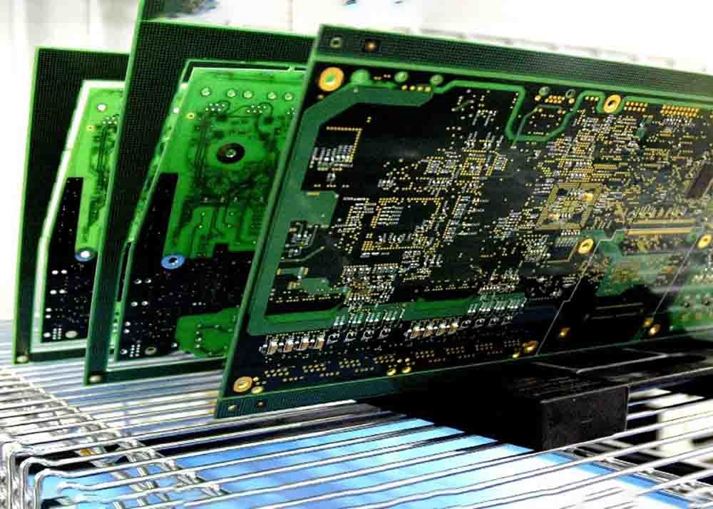
High frequency PCB are one of the widely used boards in the engineering world. These PCBs are known for their wide range of features and properties. PCBs are an integral aspect in the production of any electronics.
The use of a high frequency PCB can’t be underestimated. This circuit board has been used for the production of various electronics. In this article, we will be discussing important things you need to know about this PCB.
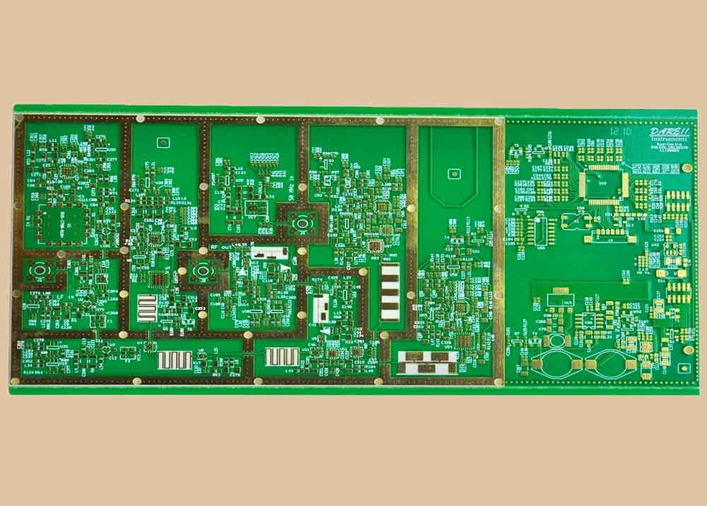
High frequency PCB transmit electromagnetic waves with minimal losses. This type of PCB is commonly utilized in applications where transmission of signals between objects is required. In the fabrication of a high frequency PCB, the use of specific materials is required.
This board features faster rates of signal flow. Its frequency range is about 100 GHZ. High frequency boards offer low levels of thermal expansion, lower DF, and lower DK. These circuit boards are commonly used for HDI technology.
High frequency PCB offer a wide range of properties. Understanding these properties helps you to understand these PCBs. These printed circuit boards are called high frequency Boards because of the properties they offer. Let us have a look at the properties of these PCBs.
Dissipation factor: frequency PCB have a low dissipation factor which falls between 0.0019 and 0.025. This value helps to ensure that the signal transmission rate isn’t affected. Low dissipation factor also enables improved signal transmission. A lower dissipation factor can help to minimize signal loss.
Low and stable dielectric constant: The dielectric constant of a high frequency PCB is lower and stable. This helps to ensure frequency transmission. This also ensures less signal delay. Lower dielectric constant leads to higher rate of frequency transmission.
Chemical resistance: High frequency PCBs can withstand chemicals. These boards can survive chemical attack when exposed to one. Due to this property, these circuit boards are less likely to corrode.
Low moisture absorption: These PCBs have a low rate of water absorption. It doesn’t absorb moisture and as such, it can withstand a humid environment.
Low dimensional stability: frequency PCB feature low dimensional stability. These PCBs maintain their size irrespective of the temperature they are exposed to. Even when they are exposed to heat, their size remains the same.
PCB designers need to take some steps when designing high frequency PCB material. Below are steps that need to be taken;
Before you commence with the PCB design, it is vital you have a design in mind. Doing this will help you to prevent anything that might cause setbacks for your design. Having a checklist is an important way to go about this.
Make sure you determine the voltage and power demands for the integrated circuits. Decide if you will be dividing any power planes. You also need to check if different signals can be accommodated. The manufacturer helps to ensure what the requirements for minimal tolerance are. It is important you have a plan of how to reduce the noise level on your high-frequency signals.
Immediately you plan how to design the PCB, it is important to write down the demands for the stack up layer. You can seek the help of the manufacturer to know the specific material for your PCBs. It is important you understand the specific constraints and materials for your printed circuit board.
When it comes to floor planning, you have to divide your PCB into sections. You need to determine if you will be placing your subcircuits into a bigger design. This is important when there are digital and analog sections that need to be carefully isolated to reduce interference.
This is an important step. After you have defined the PCB layout, you need to examine your design. You need to understand the ground plane. You may not have to divide the ground plane using a routed signal.
Dividing the ground plane indicates that you need to rotate the void. This may influence the signal timings and EMI. Dividing the ground plane is necessary. Make sure a resistor is included along the signal trace. This will help the signal have a gap which enhances the return path.
High frequency PCBs often feature small pad. Their pads are smaller than that of other PCBs. Reducing the PCB space helps to ensure the PCB is useful. You can also maintain the pad size to match the component pins size.
Reducing space comes with several benefits. This will minimize the parasitic capacitance and increase the mechanical strength. If you reduce the space, there will be more space for various pairs.
If you want to get more shielding benefits of this board, you need to route your frequency signals. High-frequency signals produce high radiation. There can be interference between two separate signals due to this. Routing the frequency signals can help you prevent this from happening.
Design a good current return path: For high frequency PCB, every signal needs a route. The route begins from the source ending at the sink via the path. Minimal obstruction is required by the path. This is an integral part of the design and fabrication of radio frequency substrates.
In some cases, you might need to utilize a via to make sure the path remains smooth. The currents will likely spread over divisions on your ground plane if you don’t do this.
Use 3W rule to reduce trace coupling: When it comes to signal integrity during transmission, line coupling may result in a serious challenge. The 3W rule will help you to reduce this. Applying this rule will ensure there is increase in the distance between the traces and as such, minimizing the coupling effect.
Apply 20H rule to reduce plane coupling: When there is coupling between ground and power planes it can be a threat to your PCB design. According to the 20H rule, you need to make sure the thickness between the adjacent power and ground plane is much thicker than the power plane.
The fabrication process of high-frequency circuit boards is a straightforward one. It is very easy to fabricate a PCB if you can understand some considerations.
Make a PCB design: This is the first thing you do. Here, you have to plan where the PCB blueprint will be placed. You can utilize Extended Gerber, designer software, to help with your design.
Print PCB design: Here, you print your PCB design. A plotter printer is used for printing. This printer produces a PCB film. This film has two ink types, the black ink and the clear ink. The clear ink shows the non-conductive areas of the PCB. The copper and the circuit of the board use the black ink.
Print copper for the inner layers: In this stage, the PCB manufacturing starts here. After printing the PCB on the laminate, the copper will be pre-bonded on the exact laminate that serves as the PCB structure. To unveil the initial PCB blueprint, the copper can be engraved.
Layers alignment: In high frequency PCB manufacturing, the layers have to be aligned. The holes can be used to arrange both the outer and inner PCB layers.
PCB layers lamination: Here, you laminate the PCB and the lay-up steps. Prepare the outer and inner layer and then join them. A metal clamp can help you join the layers.
Drilling: An X-ray machine can help you to determine the drilling spots. You can then drill holes to help secure the circuit board. The extra copper can be filed off after you complete drilling.
Plating of PCB: For PCB plating, you will need chemicals. These chemicals will help you sandwich the layers together. Ensure you clean the board before using different chemicals on it.
Solder masking: Here, the panel has to be cleaned before applying the solder mask. An epoxy ink and the solder film will be applied.
Screening and finishing of silk: The PCB will be either plated with HASL, silver, or gold. This will provide shielding to the copper and the pad. Silk screen the PCB after it has been plated.
Testing: To ensure your circuit board functions well, you are required to test it. The isolation and circuit continuity tests are an example of these tests.
Cutting: Once you have tested your PCB, you can make some cuts from your PCB panel. The PCB cutting can be done through a CNC machine or a V-a groove.
High frequency PCBs are used in various applications. These boards are specially fabricated to meet the requirements of high temperature applications. They are used in applications like;
Advanced communication system: These boards are used in the communication systems. They are commonly used in filtering devices, amplifiers, booster stations, and receivers.
Military industry: High frequency PCB materials are used in the production of ammunition and firearms.
Radar systems: These PCBs play a vital role especially in the marine and aviation industries. Radar systems prevent ships from obstacles like icebergs in marine application. The radar system guides aircraft and as such prevents accidents.
Medical systems: These boards are used in the manufacturing of medical electronics like monitoring and diagnostic devices.
High frequency PCBs offer great features that make them suitable for use in different applications. They meet the demands of high-frequency and high-performance applications. These boards are popular in the electronics industry.
Global Well Electronic Inc. is a professional PCB solution supplier from Shenzhen, China, integrating PCB circuit board production and processing, STM processing and mounting, PCBA OEM, component purchasing, PCB/PCBA custom design-production- A comprehensive PCB circuit board company with one-stop turnkey service of processing-assembly-finished products. The company has a strong supply chain system, a professional and efficient collaborative team, a sound and complete quality control system, and the business philosophy of honesty and trustworthiness, customer first, and presents the products to everyone with low prices, reliable quality, high-quality service and after-sales service. client.
We provide total PCB solutions from PCB design to final mass production, including PCB fabrication and assembly, component sourcing, solder paste stencils, conformal coatings, and more. Serving the global electronics field, including industrial control, medical electronics, military equipment, power communication, automotive electronics, AI artificial intelligence, smart home and other industries.
![]()
![]()
1. PCB fabrication.
2. Turnkey PCBA: PCB+components sourcing+SMD and through-hole assembly
3. PCB clone, PCB reverse engineering.
![]()
PCB or PCBA Files Requests:
1. Gerber files of the bare PCB board
2. BOM (Bill of material) for assembly (please kindly advise us if there is any acceptablecomponents substitution.)
3. Testing Guide & Test Fixtures if necessary
4. Programming files & Programming tool if necessary
5. Schematic if necessary
![]()
| Order Quantity | 1-300,000,30000 Square Meter/Square Meters per Month module electronic board |
| Layer | 1,2,4,6,upto 40 layer |
| Material | FR-4,glass epoxy,FR4 High Tg,Rohs compliant,Aluminum,Rogers,etc |
| PCB type | Rigid,flexible,rigid-flexible |
| Shape | Any shape: Rectangular,round,slots,cutouts,complex,irregular |
| Max PCB dimensions | 20inch*20inch or 500mm*500mm |
| Thickness | 0.2~4.0mm, Flex 0.01~0.25'' |
| Thickness tolerance | ± 10% |
| Copper thickness | 0.5-4 oz |
| Copper thickness tolerance | ± 0.25oz |
| Surface finish | HASL,Nickle,Imm Gold,Imm Tin,Imm Silver,OSP etc |
| Solder mask | Green, red,white,yellow,blue,black, Double-sided |
| Silk screen | White,yellow,black,or negative, Double-sided or single-sided |
| Silk screen min line width | 0.006'' or 0.15mm |
| Min drill hole diameter | 0.01'',0.25mm.or 10 mil |
| Min trace/gap | 0.075mm or 3mil |
| PCB cutting | Shear,V-score,tab-routed |
| Turnkey PCBA | PCB+components sourcing+assembly+package |
| Assembly details | SMT and Thru-hole, ISO lines |
| Lead Time | Prototype: 15 work days. Mass order: 20~25 work days |
| Testing on products | Flying Probe Test, X-ray Inspection, AOI Test, functional test |
| Quantity | Min quantity: 1pcs. Prototype, small order, mass order, all OK |
| Files we need | PCB: Gerber files(CAM, PCB, PCBDOC) |
| Components: Bill of Materials(BOM list) | |
| Assembly: Pick-N-Place file | |
| PCB panel Size | Min size: 0.25*0.25 inches(6*6mm) |
| Max size: 20*20 inches(500*500mm) | |
| PCB Solder Type | Water Soluble Solder Paste, RoHS lead free |
| Components details | Passive Down to 0201 size |
| BGA and VFBGA | |
| Leadless Chip Carriers/CSP | |
| Double-sided SMT Assembly | |
| Fine Pitch to 0.8mils | |
| BGA Repair and Reball | |
| Part Removal and Replacement | |
| Component package | Cut Tape,Tube,Reels,Loose Parts |
| PCBA process |
Drilling-----Exposure-----Plating-----Etaching Stripping-----Punching-----Electrical Testing-----SMT-----Wave Soldering-----Assembling-----ICT-----Function Testing-----Temperature - Humidity Testing |
![]()
![]()
![]()
![]()
![]()
![]()
![]()
![]()
Packing details:
PCBA are packed into plastic bags. Plastic bags are put into small carton. 4 small carton into a big carton.
A big carton: 35×32×40 cm size.
Shipping Express:
FedEx, DHL, UPS, TNT, EMS, private lines, etc.
Air freight, Sea shipping
![]()
If you need help on PCB layout, you can contact us and send the board to us. We also provide Reverse Engineering Service.
We have been providing PCB Manufacture for many years in China,and we have rich experience in product production and product assembly.We believe our team will provide high quality and low cost service for you.
Thank you very much for all your support .
Best Regareds.


