

A high-frequency PCB can meet your needs when incorporating a special signal requirement into your electronic components and products. It offers a frequency range of 500MHz - 2GHz, making it ideally suited for high-speed designs, as well as radio frequency (RF), microwave and mobile applications. These higher transmission frequencies can also provide the faster signal flow rates that are a necessity in today's increasingly complex electronic switches and other components.
A High-Frequency PCB Requires the Use of Specialized Materials
Special materials are required to achieve the high frequency provided by this type of printed circuit board - any changes in the Er value of these materials can affect the impedance of the board. Many PCB designers turn to Rogers dielectric material for its lower dielectric loss, reduced signal loss, lower cost of circuit fabrication and better suitability for fast-turnaround prototyping applications.
Apart from choosing the appropriate PCB material and determining the correct the value of the Er, designers should take parameter such as conductor width and spacing, substrate constant into consideration. These parameters must be exactly specified and implemented with the highest level of process control.
PCBCart is an experienced full service PCB manufacturer who provides a reliable, superior-performing high-frequency PCB fab services.
We manufacture high-frequency PCBs with frequency typically in the range from 500MHz to 2GHz. The following table shows some of our common-use materials for High-Frequency PCBs.
| Material | Dielectric Constant |
| RO4350B | 3.48±0.05@10 GHz |
| RO4003C | 3.38±@10 GHz |
| Ro3003 | 3.00±0.04@10 GHz |
| Ro3010 | 10.2±0.03@10 GHz |
| RT5880 | 2.20±0.02@10 GHz |
Global Well Electronic Inc. is a professional PCB solution supplier from Shenzhen, China, integrating PCB circuit board production and processing, STM processing and mounting, PCBA OEM, component purchasing, PCB/PCBA custom design-production- A comprehensive PCB circuit board company with one-stop turnkey service of processing-assembly-finished products. The company has a strong supply chain system, a professional and efficient collaborative team, a sound and complete quality control system, and the business philosophy of honesty and trustworthiness, customer first, and presents the products to everyone with low prices, reliable quality, high-quality service and after-sales service. client.
We provide total PCB solutions from PCB design to final mass production, including PCB fabrication and assembly, component sourcing, solder paste stencils, conformal coatings, and more. Serving the global electronics field, including industrial control, medical electronics, military equipment, power communication, automotive electronics, AI artificial intelligence, smart home and other industries.
![]()
![]()
1. PCB fabrication.
2. Turnkey PCBA: PCB+components sourcing+SMD and through-hole assembly
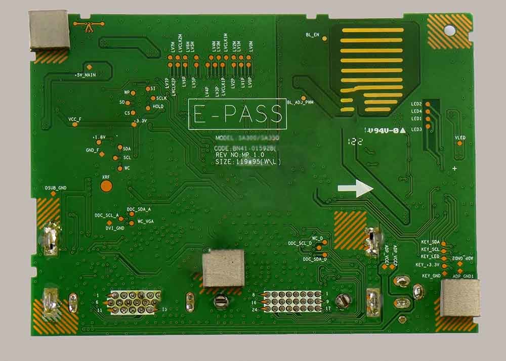
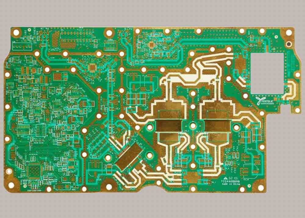
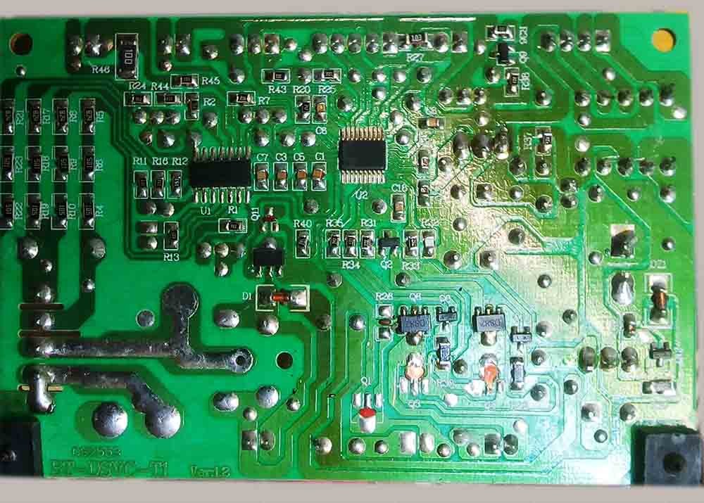
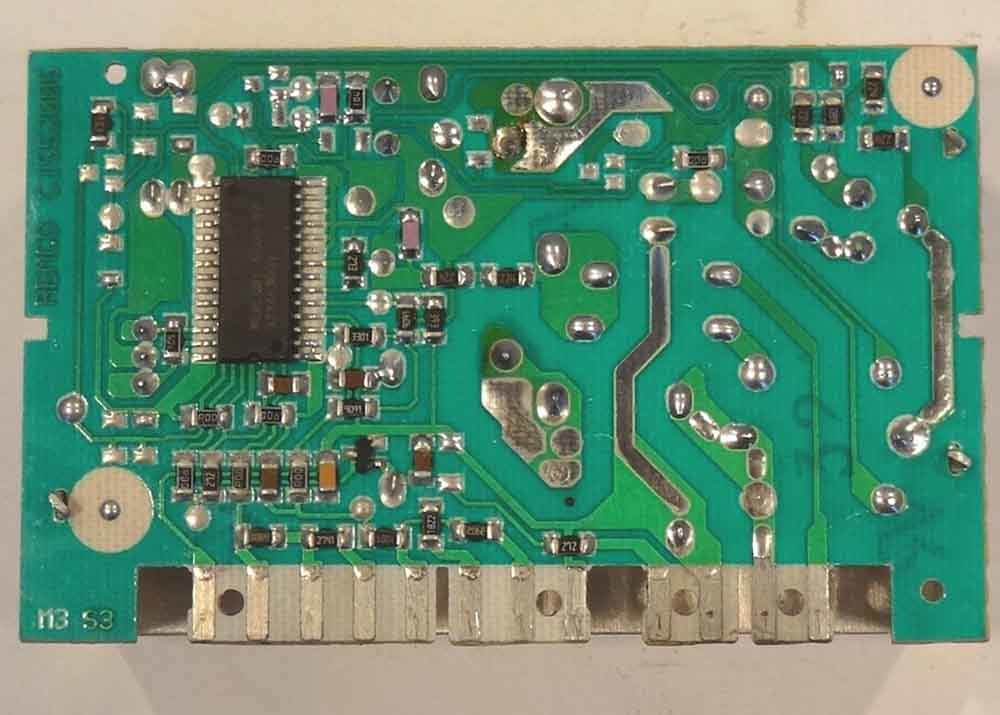
3. PCB clone, PCB reverse engineering.
![]()
PCB or PCBA Files Requests:
1. Gerber files of the bare PCB board
2. BOM (Bill of material) for assembly (please kindly advise us if there is any acceptablecomponents substitution.)
3. Testing Guide & Test Fixtures if necessary
4. Programming files & Programming tool if necessary
5. Schematic if necessary
![]()
| Order Quantity | 1-300,000,30000 Square Meter/Square Meters per Month module electronic board |
| Layer | 1,2,4,6,upto 40 layer |
| Material | FR-4,glass epoxy,FR4 High Tg,Rohs compliant,Aluminum,Rogers,etc |
| PCB type | Rigid,flexible,rigid-flexible |
| Shape | Any shape: Rectangular,round,slots,cutouts,complex,irregular |
| Max PCB dimensions | 20inch*20inch or 500mm*500mm |
| Thickness | 0.2~4.0mm, Flex 0.01~0.25'' |
| Thickness tolerance | ± 10% |
| Copper thickness | 0.5-4 oz |
| Copper thickness tolerance | ± 0.25oz |
| Surface finish | HASL,Nickle,Imm Gold,Imm Tin,Imm Silver,OSP etc |
| Solder mask | Green, red,white,yellow,blue,black, Double-sided |
| Silk screen | White,yellow,black,or negative, Double-sided or single-sided |
| Silk screen min line width | 0.006'' or 0.15mm |
| Min drill hole diameter | 0.01'',0.25mm.or 10 mil |
| Min trace/gap | 0.075mm or 3mil |
| PCB cutting | Shear,V-score,tab-routed |
| Turnkey PCBA | PCB+components sourcing+assembly+package |
| Assembly details | SMT and Thru-hole, ISO lines |
| Lead Time | Prototype: 15 work days. Mass order: 20~25 work days |
| Testing on products | Flying Probe Test, X-ray Inspection, AOI Test, functional test |
| Quantity | Min quantity: 1pcs. Prototype, small order, mass order, all OK |
| Files we need | PCB: Gerber files(CAM, PCB, PCBDOC) |
| Components: Bill of Materials(BOM list) | |
| Assembly: Pick-N-Place file | |
| PCB panel Size | Min size: 0.25*0.25 inches(6*6mm) |
| Max size: 20*20 inches(500*500mm) | |
| PCB Solder Type | Water Soluble Solder Paste, RoHS lead free |
| Components details | Passive Down to 0201 size |
| BGA and VFBGA | |
| Leadless Chip Carriers/CSP | |
| Double-sided SMT Assembly | |
| Fine Pitch to 0.8mils | |
| BGA Repair and Reball | |
| Part Removal and Replacement | |
| Component package | Cut Tape,Tube,Reels,Loose Parts |
| PCBA process |
Drilling-----Exposure-----Plating-----Etaching Stripping-----Punching-----Electrical Testing-----SMT-----Wave Soldering-----Assembling-----ICT-----Function Testing-----Temperature - Humidity Testing |
![]()
![]()
![]()
![]()
![]()
![]()
![]()
![]()
Packing details:
PCBA are packed into plastic bags. Plastic bags are put into small carton. 4 small carton into a big carton.
A big carton: 35×32×40 cm size.
Shipping Express:
FedEx, DHL, UPS, TNT, EMS, private lines, etc.
Air freight, Sea shipping
![]()
If you need help on PCB layout, you can contact us and send the board to us. We also provide Reverse Engineering Service.
We have been providing PCB Manufacture for many years in China,and we have rich experience in product production and product assembly.We believe our team will provide high quality and low cost service for you.
Thank you very much for all your support .
Best Regareds.


