

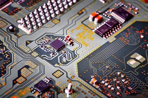
With the development of electronic technology, there is a great demand on high speed PCB design to work. Because they can work with integrated circuits at high speeds for most electronic devices, even quite simple ones. When you design a high speed PCB, it needs to take some factors and parameters into consideration. What’s more, you will find that the basic PCB design rules and methods you have mastered is what you need to learn. Needless to say, it will be of great assistance to PCB designers in high speed PCB design.
High speed PCB design is any design where the integrity of your signals begins to be impacted by physical characteristics of your PCB, such as layout, packaging, interconnection, as well as layer stackup and so on. What’s more, you will come into the world of high speed PCB design when you start to design the boards and get into troubles such as delays, crosstalk, reflections, or emissions.
High speed design is so unique because of the attention paid to these issues. You might be used to designing a simple PCB where you are mainly in paying attention to component placement and routing. However, it’s more important to take some factors into consideration when using a high speed design, such as how close they are to signals, what width they are going to be, where you are placing the traces, as well as what kinds of components they are connected. What’s more, it will achieve a great level for your PCB design process when you take the factors into considerations.
![]()
1. Know a design software that can offer advanced options
It needs a lot of complex features for high speed designs in your CAD software. What’s more, there may not have many programs for hobbyists, and usually it doesn’t have advanced options based on Web suites. So you need to have a better understanding of a power, CAD tool.
2. High speed routing
When it comes to high speed traces, a designer needs to know the rules for essential routing, including not cutting ground planes and keeping trails short. So prevent digital lines a certain distance from crosstalk, and shield any interference creating elements so that damaging the signal integrity.
3. Routing traces with impedance control
It needs impedance matching for some types of signals which are about 40-120 ohms. And characteristic impedance matched hints are antennae and many differential pairs.
It’s important for designer to know how to calculate trace width and layer stack for necessary impedance values. If there is not correct impedance values, it may make a serious effect on signal, which will lead to data corruption.
4. Length matching traces
There are many lines in high speed memory buses and interface buses. The lines can work at quite high frequency, so it’s vital that the signals need to be from the transmitting terminal to the receiving terminal at the same time. What’s more, it needs to a feature called length matching. So most common standards define tolerance values that need to match length.
![]()
5. Minimizing loop area
There are some tips high speed PCB designers need to know that high frequency signals will lead to some problems of EMI, EMC. So they need to abide by basic rules such as having continuous ground planes and reducing loop areas with optimizing current return paths for traces, as well as putting in many stitching vias.
High speed PCB design considerations
PCB layout is so important
Needless to say, it’s important for final results to have an efficient PCB fabrication in high speed circuitry. However, there is not PCB layout at first to take into consideration in the process. So there will have a great effect on design so that achieve the necessary functionality and succeed in PCB fabrication, such as advanced planning and abidance by significant factors. What’s more, you need to deal with the issues before PCB layout, such as the practices of designing for manufacturing (DFM) and taking extra account for high speed PCB demands.
When it begins to test or use in PCB fabrication, poor layouts can lead to performance issues. What’s worse, it will need to spend more cost and time on redesigning or reworking because evaluating the PCB failures or performance issues and reassembling prototype layouts.
Considerations for PCB design
In fact, high speed PCB design has a lot of limits for designer, because you need to meet the demands of various signal speeds and other designs. So it needs to take some factors into consideration if achieving designing the board in high speed circuitry as follows:
Schematic considerations:as you know, a great schematic can lay a good foundation for PCB design. So you can treat the schematic differently according to whether you are an PCB designer or electrical engineer. In general, it treats the schematic as a communication way that can connect to the board. But schematic can make a great effect on organizing and presenting your high speed design. So there are much available information as possible on the design schematic such as trace lengths, necessary component placements, the information of PCB manufacturer and so on.
Trace length tuning: you need to tune the length of the traces to synchronize signal transmission with data lines when you use a high speed interface. However the interface may fail at the maximum frequency or will not work at all as it’s not synchronized. What’s more, the higher the frequency of the interface is, the higher the length matching demands are. So you just need to tune the lengths of all traces in case of a parallel interface. It’s important to look into tuning those trace lengths to get the desired lengths within a group of signals.
PCB materials and stack-up demands for high speed: there will have an effect on your high speed design, such as how the layer stack-up is structured and what materials your PCB is built from.
High speed placement strategies: it can optimize the component placement with various methods for high speed design, as well as improve the component footprint enhancements to achieve high speed, because changing pad dimensions and component clearances can make an effect on minimizing high speed connection lengths.
Differential pair and trace length routing: it’s so important to have the routing of differential pairs in a high speed design so that there is paired signals making it at the same time.
![]()
Crosstalk, impedance control, and parallelism considerations: there are many various forces making a bad effect on your design in high speed design. What’s more, it needs to take some tips into consideration, for example how to minimize the influence on your design.
Understanding stripline and microstrip: in general, it needs to have a various method to routing traces for high speed designs. If you want to achieve high speed routing, you’d better have a better understanding of stripline and microstrip routing techniques.
Routing topologies and best routing practices: in general, if you want to achieve the necessary circuit path for high speed routing, it needs to use specific shapes or topologies. What’s more, it is great to explore various methods to route with trace lengths, escapes, return paths and so on.
Simulators: it has a great benefit from simulation both before the layout starts, during and afterward for high speed designs. So you should have a better understanding of your PCB design software to learn the tips and tricks used to simulate your designs.
How to know if you need a high speed design?
1. It there high speed interface in your board?
A fast method to find out if you need to abide by high speed design guidelines is to check whether you have high speed interfaces, for example DDR, PCI-e, or even video interfaces like DVI, HDMI and so on.
There are some high speed design rules you need to follow for all these interfaces. What’s more, offer the accurate specifications of each data in the documentation.
2. The ratio of your trace length to the wavelength of signals
In general, your PCB will certainly need a high speed design if the wavelength of your message is the same as the trace length. Because some standards such as DDR require traces that have a length matched to minimal tolerances.
A great rough figure is that if your trace length and wavelength can control within one order of each other. Then you’d better check the high speed designs.
![]()
3. PCB with wireless interfaces
As you know, each PCB has an antenna, it needs to design for high speed signals no matter what through the connector or on the board. What’s more, onboard antennas also require close impedance to match tune length.
It will need to connect to the connectors that have a specific impedance value for circuit boards with SMA connectors or similar.
In a word, learning about high speed PCB design is leaning about a different engineering filed. Although there are a lot of factors you need to take into consideration when working on a high speed design. Luckily, your CAD software for PCB design will give a hand to you, such as impedance calculators, trace length reporting options, differential pair routers, as well as other tools.
1. PCB fabrication.
2. Turnkey PCBA: PCB+components sourcing+SMD and through-hole assembly
Global Well Electronic Inc. is a professional PCB solution supplier from Shenzhen, China, integrating PCB circuit board production and processing, STM processing and mounting, PCBA OEM, component purchasing, PCB/PCBA custom design-production- A comprehensive PCB circuit board company with one-stop turnkey service of processing-assembly-finished products. The company has a strong supply chain system, a professional and efficient collaborative team, a sound and complete quality control system, and the business philosophy of honesty and trustworthiness, customer first, and presents the products to everyone with low prices, reliable quality, high-quality service and after-sales service. client.
We provide total PCB solutions from PCB design to final mass production, including PCB fabrication and assembly, component sourcing, solder paste stencils, conformal coatings, and more. Serving the global electronics field, including industrial control, medical electronics, military equipment, power communication, automotive electronics, AI artificial intelligence, smart home and other industries.
![]()
Our factory located in Shenzhen, and have almost 300
employees, more than 30 production lines include SMT, DIP, automatic welding, aging test and assembly. We have SMT machines from Japan and Korea, automatic solder paste printing machines, solder paste inspection machine(SPI)12 temperature zone reflow soldering machine, AOI detector, X-RAY detector, wave soldering machine, EM PCB ,dispenser,laser print machine etc., Different line configurations can meet requirements from small sample order to bulk shipment.
Our company has obtained ISO 9001 quality system certification and ISO 14001 system certification. With multi-testingprocedures, our products carry out the quality system standard strictly.
![]()
![]()
![]()
![]()
![]()
| Order Quantity | 1-300,000,30000 Square Meter/Square Meters per Month module electronic board |
| Layer | 1,2,4,6,upto 24 layer |
| Material | FR-4,glass epoxy,FR4 High Tg,Rohs compliant,Aluminum,Rogers,etc |
| PCB type | Rigid,flexible,rigid-flexible |
| Shape | Any shape: Rectangular,round,slots,cutouts,complex,irregular |
| Max PCB dimensions | 20inch*20inch or 500mm*500mm |
| Thickness | 0.2~4.0mm, Flex 0.01~0.25'' |
| Thickness tolerance | ± 10% |
| Copper thickness | 0.5-4 oz |
| Copper thickness tolerance | ± 0.25oz |
| Surface finish | HASL,Nickle,Imm Gold,Imm Tin,Imm Silver,OSP etc |
| Solder mask | Green, red,white,yellow,blue,black, Double-sided |
| Silk screen | White,yellow,black,or negative, Double-sided or single-sided |
| Silk screen min line width | 0.006'' or 0.15mm |
| Min drill hole diameter | 0.01'',0.25mm.or 10 mil |
| Min trace/gap | 0.075mm or 3mil |
| PCB cutting | Shear,V-score,tab-routed |
| Turnkey PCBA | PCB+components sourcing+assembly+package |
| Assembly details | SMT and Thru-hole, ISO lines |
| Lead Time | Prototype: 15 work days. Mass order: 20~25 work days |
| Testing on products | Flying Probe Test, X-ray Inspection, AOI Test, functional test |
| Quantity | Min quantity: 1pcs. Prototype, small order, mass order, all OK |
| Files we need | PCB: Gerber files(CAM, PCB, PCBDOC) |
| Components: Bill of Materials(BOM list) | |
| Assembly: Pick-N-Place file | |
| PCB panel Size | Min size: 0.25*0.25 inches(6*6mm) |
| Max size: 20*20 inches(500*500mm) | |
| PCB Solder Type | Water Soluble Solder Paste, RoHS lead free |
| Components details | Passive Down to 0201 size |
| BGA and VFBGA | |
| Leadless Chip Carriers/CSP | |
| Double-sided SMT Assembly | |
| Fine Pitch to 0.8mils | |
| BGA Repair and Reball | |
| Part Removal and Replacement | |
| Component package | Cut Tape,Tube,Reels,Loose Parts |
| PCBA process |
Drilling-----Exposure-----Plating-----Etaching Stripping-----Punching-----Electrical Testing-----SMT-----Wave Soldering-----Assembling-----ICT-----Function Testing-----Temperature - Humidity Testing |
![]()
![]()
![]()
![]()
![]()
Packing details:
PCBA are packed into plastic bags. Plastic bags are put into small carton. 4 small carton into a big carton.
A big carton: 35×32×40 cm size.
Shipping Express:
FedEx, DHL, UPS, TNT, EMS, private lines, etc.
Air freight, Sea shipping
![]()
If you need help on PCB layout, you can contact us and send the board to us. We also provide Reverse Engineering Service.
We have been providing PCB Manufacture for many years in China,and we have rich experience in product production and product assembly.We believe our team will provide high quality and low cost service for you.
Thank you very much for all your support .
Best Regareds.
1. Gerber files of the bare PCB board
2. BOM (Bill of material) for assembly (please kindly advise us if there is any acceptablecomponents substitution.)
3. Testing Guide & Test Fixtures if necessary
4. Programming files & Programming tool if necessary
5. Schematic if necessary
A: Gerber or Eagle, BOM listing, PNP and Components Position
A: Yes, we can custom you sample to test before mass production
A: Within 6 hours for PCB quotation and around 24 hours for PCBA quotation.
A: 7-10 days for PCB production and components purchasing, and 10 days for PCB assembly and Testing


