
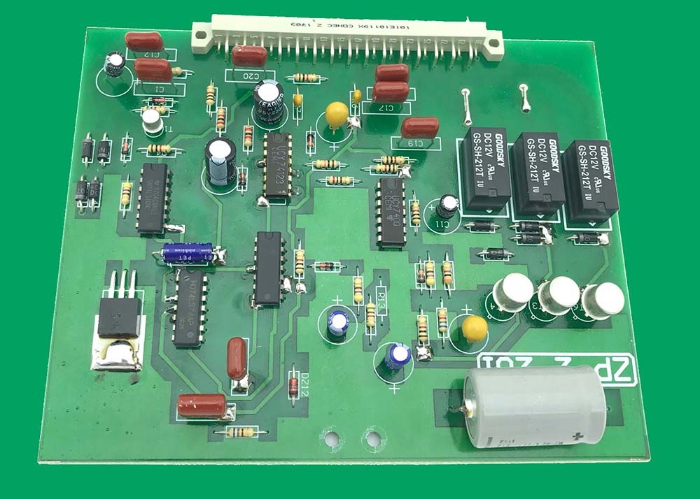
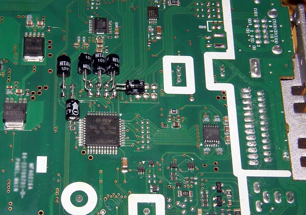
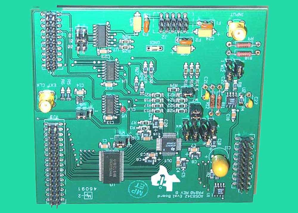
In the making process of printed circuit boards the surface of the board is coated with copper. All electric connections depend upon the conductivity of the copper. On the other hand, the copper is also highly chemically reactive, when it exposed to the moisture of atmosphere it oxidizes abruptly. As a result high temperature requirement for soldering and ultimately it affect the end product reliability. Therefore there is need aroused for surface finishing of boards. The employment of surface finish coating serve two purposes, the first is to protect copper from oxidizing and another is to provide a surface which can maintain it quality after soldering and during assembly of various components with printed circuit boards.
here are various types of surface finishes available which involves various chemical substances, like: Hot air soldering leveling, Immersion in Tin/silver, OSP and ENIG. Among all these processes of surface finishing OSP has turned out to be a low cost process and environment friendly.
OSP abbreviated as “Organic Solderability Preservative” . At the time of surface finishing of board it refers to a organic layer, which adhere with the copper by means of adsorption. Being organic it is permanent wall to prevent oxidation of copper, thermal shocks moisture. This organic coating also gives easy removal or less deposition of flux during soldering and ultimately helps to reduce the soldering time of assembly process of printed circuit board.
The major point is the low cost and easy processing makes this process of surface finishing more popular across the printed circuit board industry. Few advantages are enlisted below:
1. Simple PCB Manufacturing process: Printed circuit boards coated with OSP are easy to rework and maintain. Therefore, it is an advantage for PCB manufacturers to repair the surface finish coating with less time and cost, once coating found damaged.
2. OSP coated boards gives good performance in terms of solder wetting and joining between flux, vias and pads.
3. Because of application of water based compound in OSP surface finishing, makes it environment friendly. Therefore this can be termed as a green electronic product which is catering to the green regulations.
4. Implementation of simple chemical compound and less complexity of process it is of low cost. With most of the chemicals of OSP there is no need of solder mask ink. But some chemicals require a little proportion of solder mask ink in some special cases.
5. Storage time is long for the printed circuit board if coated with OSP. It is implemented with single-side SMT assembly as well as double sided prototype pcb assembly.
Storage Requirement: The coating generated by OSP surface finish is quite thin. Therefore, care must be taken, when printed circuit in operation or is being transported. If board with OSP surface finish is exposed to the open atmosphere and humidity, then there are chances that oxidation will possibly damage the surface of printed circuit board, and then it leads to further consequences ahead in the process of assembly and its functioning.
The process for manufacturing OSP has three stages: oil removal, micro-corrosion, and film formation.
Stage 1: Oil Removal
Removing all the contaminants and oil is crucial if you want a high-quality protective film. Otherwise, you’ll end up with an uneven film.
Luckily, there are ways you can avoid uneven films. First, you’ll need to control the concentration of your oil removal solution. Then, inspect the process to see if it’s okay.
If you notice that the effects of your oil removal are poor, you’ll need to replace it fast with chemicals specifically for this purpose.
Step 2: Micro-corrosion
Micro-corrosion aims to create a natural copper surface. Also, it directly influences how fast your OSP forms. Additionally, it’s vital to control the micro-corrosion thickness if you want a stable film thickness.
Also, the acceptable range for maintaining micro-corrosion is between 1.0um to 1.5um. Once you have your maintenance values, it’s easy to measure the micro-corrosion rate.
Step 3: Film Formation
It’s crucial to use DI washing before and after forming your film. Also, you must limit the solution’s PH between 4.0 and 7.0. Otherwise, you’ll contaminate the solution for film formation.
Here’s where the OSP process gets tricky. First, you need to control the film’s thickness so it doesn’t affect your welding performance. The ideal thickness can be anywhere between 0.2um and 0.5um.
Note: the thinner your film is, the lesser OSP advantages you’ll get. For instance, you may get lesser thermal shock capacity or oxidation protection. Also, remember to use DI washing after forming your film.
1. PCB fabrication.
2. Turnkey PCBA: PCB+components sourcing+SMD and through-hole assembly
3. PCB clone, PCB reverse engineering.
PCB or PCBA Files Requests:
1. Gerber files of the bare PCB board
2. BOM (Bill of material) for assembly (please kindly advise us if there is any acceptablecomponents substitution.)
3. Testing Guide & Test Fixtures if necessary
4. Programming files & Programming tool if necessary
5. Schematic if necessary
Global Well Electronic Inc. is a professional PCB solution supplier from Shenzhen, China, integrating PCB circuit board production and processing, STM processing and mounting, PCBA OEM, component purchasing, PCB/PCBA custom design-production- A comprehensive PCB circuit board company with one-stop turnkey service of processing-assembly-finished products. The company has a strong supply chain system, a professional and efficient collaborative team, a sound and complete quality control system, and the business philosophy of honesty and trustworthiness, customer first, and presents the products to everyone with low prices, reliable quality, high-quality service and after-sales service. client.
We provide total PCB solutions from PCB design to final mass production, including PCB fabrication and assembly, component sourcing, solder paste stencils, conformal coatings, and more. Serving the global electronics field, including industrial control, medical electronics, military equipment, power communication, automotive electronics, AI artificial intelligence, smart home and other industries.
![]()
Our factory located in Shenzhen, and have almost 300 employees, more than 30 production lines include SMT, DIP, automatic welding, aging test and assembly. We have SMT machines from Japan and Korea, automatic solder paste printing machines, solder paste inspection machine(SPI)12 temperature zone reflow soldering machine, AOI detector, X-RAY detector, wave soldering machine, EM PCB ,dispenser,laser print machine etc., Different line configurations can meet requirements from small sample order to bulk shipment.
Our company has obtained ISO 9001 quality system certification and ISO 14001 system certification. With multi-testingprocedures, our products carry out the quality system standard strictly.
![]()
![]()
| Order Quantity | 1-300,000,30000 Square Meter/Square Meters per Month module electronic board |
| Layer | 1,2,4,6,upto 24 layer |
| Material | FR-4,glass epoxy,FR4 High Tg,Rohs compliant,Aluminum,Rogers,etc |
| PCB type | Rigid,flexible,rigid-flexible |
| Shape | Any shape: Rectangular,round,slots,cutouts,complex,irregular |
| Max PCB dimensions | 20inch*20inch or 500mm*500mm |
| Thickness | 0.2~4.0mm, Flex 0.01~0.25'' |
| Thickness tolerance | ± 10% |
| Copper thickness | 0.5-4 oz |
| Copper thickness tolerance | ± 0.25oz |
| Surface finish | HASL,Nickle,Imm Gold,Imm Tin,Imm Silver,OSP etc |
| Solder mask | Green, red,white,yellow,blue,black, Double-sided |
| Silk screen | White,yellow,black,or negative, Double-sided or single-sided |
| Silk screen min line width | 0.006'' or 0.15mm |
| Min drill hole diameter | 0.01'',0.25mm.or 10 mil |
| Min trace/gap | 0.075mm or 3mil |
| PCB cutting | Shear,V-score,tab-routed |
| Turnkey PCBA | PCB+components sourcing+assembly+package |
| Assembly details | SMT and Thru-hole, ISO lines |
| Lead Time | Prototype: 15 work days. Mass order: 20~25 work days |
| Testing on products | Flying Probe Test, X-ray Inspection, AOI Test, functional test |
| Quantity | Min quantity: 1pcs. Prototype, small order, mass order, all OK |
| Files we need | PCB: Gerber files(CAM, PCB, PCBDOC) |
| Components: Bill of Materials(BOM list) | |
| Assembly: Pick-N-Place file | |
| PCB panel Size | Min size: 0.25*0.25 inches(6*6mm) |
| Max size: 20*20 inches(500*500mm) | |
| PCB Solder Type | Water Soluble Solder Paste, RoHS lead free |
| Components details | Passive Down to 0201 size |
| BGA and VFBGA | |
| Leadless Chip Carriers/CSP | |
| Double-sided SMT Assembly | |
| Fine Pitch to 0.8mils | |
| BGA Repair and Reball | |
| Part Removal and Replacement | |
| Component package | Cut Tape,Tube,Reels,Loose Parts |
| PCBA process |
Drilling-----Exposure-----Plating-----Etaching Stripping-----Punching-----Electrical Testing-----SMT-----Wave Soldering-----Assembling-----ICT-----Function Testing-----Temperature - Humidity Testing |
![]()
![]()
Packing details:
PCBA are packed into plastic bags. Plastic bags are put into small carton. 4 small carton into a big carton.
A big carton: 35×32×40 cm size.
Shipping Express:
FedEx, DHL, UPS, TNT, EMS, private lines, etc.
Air freight, Sea shippingIf you need help on PCB layout, you can contact us and send the board to us. We also provide Reverse Engineering Service.
![]()
We have been providing PCB Manufacture for many years in China,and we have rich experience in product production and product assembly.We believe our team will provide high quality and low cost service for you.
Thank you very much for all your support .
Best Regareds.
Q: What files do you use in PCBA fabrication?
A: Gerber or Eagle, BOM listing, PNP and Components Position
Q:Is it possible you could offer sample?
A: Yes, we can custom you sample to test before mass production
Q: When will I get the quotation after sent Gerber, BOM and test procedure?
A: Within 6 hours for PCB quotation and around 24 hours for PCBA quotation.
Q: How can I know the process of my PCBA production?
A: 7-10 days for PCB production and components purchasing, and 10 days for PCB assembly and Testing
Q: How can I make sure the quality of my PCBA?
A: We ensure that each piece of PCBA products work well before shipping. We'll test all of them according to your test procedure. Also if there are any defect items during the shipping, we also can be free to repair for you.


